Part 0: Introduction
Why Learn FPGA programming?
Similar to programming, hardware design is an important pillar of fully understanding computing technology, but often programmers struggle to grasp hardware concepts because they are less accessible and require specialized tools and knowledge. ASIC design is costly and complex, while breadboards and physical circuitry come with steep learning curves and a more hands-on approach that can feel distant from the software development process. The beautiful thing about FPGAs is that they provide a perfect intersection between programming and hardware, allowing users to literally create hardware using HDL programming languages.
My Approach
When I initially learned how to program, I found that I learned best by directly applying knowledge in the form of mini projects, solidifying the concept of each abstraction from the ground up. I will attempt to do the same with FPGA programming, documenting my progress on here step by step.
I will structure each part as follows:
- Title: self explanatory
- WHW: (W)hat is this, (H)ow does it work at high level, and (W)hy does it exist?
- My implementation: Some snippets of my code, and further description of how stuff works, on a slightly lower level.
Info and Key Assumptions:
I will be using VHDL for this, and simulating my code on Vivado. I have a computer science background, so I already have knowledge of logic gates, bitwise operations, and basic computer architecture. I assume the reader should have a similar understanding, but if not, I encourage you to check out these resources:
- Geeks4Geeks Introduction to Logic Gates
- Wikipedia Logic Gates
- CodeProject.com Intro to Bitwise Operators
Quick tip: If you've played Minecraft before, building basic logic gates in minecraft really helped me understand them a lot better, I definitely recommend.
Disclaimer: Everything on this site except for the links to other resources is my own. Feel free to use it however you want.
Part 1: Getting Started, Creating a Half Adder
In this first section, I will be very specific about rudimentary things by breaking down each piece of code, walking through usage of Vivado, explaining what a test bench is, etc. because this is the first project and I want to make sure we're on the same page. As we continue in further projects, I'll assume an understanding of this stuff and not cover it as much.
What is this?
A half adder is a circuit that adds two bits together.
How does it work?
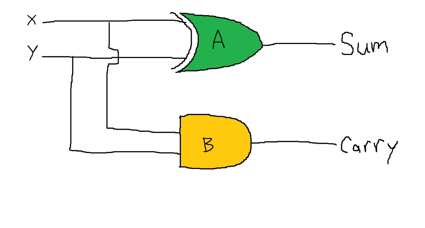
It works by taking two bits X and Y as input. It consists of an AND gate (B) and an XOR gate (A). The AND gate handles the carry, because the only way a bitwise operation can have a carry is if both bits are 1, which can be checked with an AND gate. The XOR gate handles the sum, which works because a 1 and 1 bitwise addition makes 0, as does a 0 and 0, so the only resulting 1's occur from 0,1 or 1,0, which can be captured with XOR.
I drew this in paint, but you could probably find a more clear version on the internet somewhere else.

Why does it exist?
This is fundamental for adding any number using binary (and subsequently, one way of doing multiplication). A slightly more complex version of this (full adder, covered below) is the fundamental unit of addition for the ALU. In an ALU, if you put a bunch of full adders together, let's say N full adders, that makes an N-bit adder which can do addition on numbers sized up to (2^N)-1.
Implementation
We will have two files. One for the actual FPGA code named main.vhd, and another named main_tb to test it (typically called a test bench). Let's focus on main.
Main File (main.vhd)
First, we import our libraries. This is standard to our code.
library IEEE;
use IEEE.STD_LOGIC_1164.ALL;
We then declare our inputs and outputs by using the entity keyword. We use in std_logic for inputs and out std_logic for outputs.
entity main is
port(
    X, Y : in std_logic;
    Sum, Carry : out std_logic
);
end main;
Now, it's time to declare the architecture. This contains the actual logic of our implementation, and it's where we'll do our XORing and ANDing.
architecture Behavioral of main is
begin
Sum <= X xor Y;
Carry <= X and Y;

end Behavioral;
Now we're done with our implementation. Let's move on to our test bench.
Test Bench File (main_tb.vhd)
Again, we declare our libraries. (Vivado actually did this for me)
library IEEE;
use IEEE.STD_LOGIC_1164.ALL;
Here is where the ports are usually declared, but we don't usually do this in our test bench. This is because any inputs we need will be generated within this file.
By the way, comments contain a "--" at the beginning.
entity main_tb is
-- no ports set
end main_tb;
Now, we set the architecture, which in this case is essentially just connecting this test bench file to the main file we made previously.
architecture Behavioral of main_tb is
component main
port(
    X: in std_logic;
    Y : in std_logic;
    Sum : out std_logic;
    Carry : out std_logic
);
end component;
Now, let's initialize our signals, which is what's filling in for the ports that are not declared above.
signal X: std_logic := '0';
signal Y : std_logic := '0';

signal Sum : std_logic;
signal Carry : std_logic;
At this point all we have left to do is test each possible test case. For every test case we will set X and Y, then wait a small amount of time, then move to the next case.
begin

uut: main port map (
X => X,
Y => Y,
Sum => Sum,
Carry => Carry
);

stim : process
begin
-- test 1 (00 -> s=0, c=0)
X <= '0';
Y <= '0';
wait for 10 ns;

-- test 2 (01 -> s=1, c=0)
X <= '0';
Y <= '1';
wait for 10 ns;

-- test 3 (10 -> s=1, c=0)
X <= '1';
Y <= '0';
wait for 10 ns;

-- test 4 (11 -> s=0, c=1)
X <= '1';
Y <= '1';
wait for 10ns;

wait;

end process;


end Behavioral;
That's it for the code! Now, we can simulate it in Vivado by clicking Run Simulation on the left, in the Flow Navigator menu.
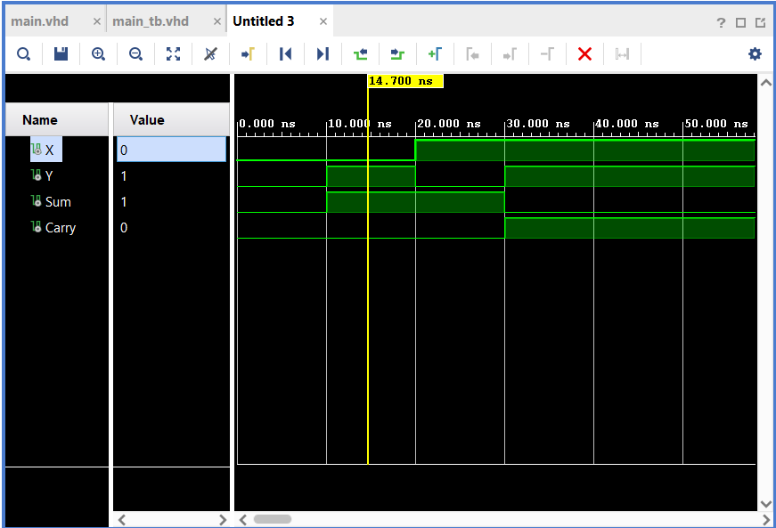
There are a lot of knobs and dials in Vivado, but all we care about right now is this part.

Note: you might need to zoom out a lot to see the waveforms because mine was zoomed way in by default.
On the right here, all of these green lines represent the state of our variables, which are on the left. Notice how at 10 nanoseconds (ns), the state changes to where Y is solid, Sum is solid, and the rest remain flat. This means that Y turned from 0 to 1, and Sum turned from 0 to 1. This equates to 0 + 1 = 1, with no carry. This is correct.
As you can see, the rest of the tests had correct results as well. You can click on each state with your mouse and the variables on the left will change accordingly.
Part 2: Full Adder
What is this?
A full adder is just a half adder with the ability to add a carry in. Think of it as the official adder. It can be linked together with other full adders to do some actual useful stuff.
How does it work?

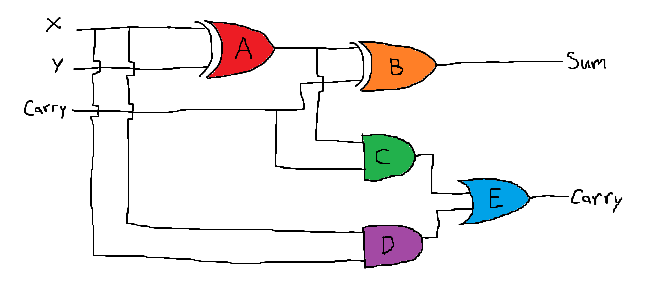
It has three inputs, X, Y and Carry_in. It contains two XOR gates, two AND gates, and one OR gate. Allow me to explain each one:
- gate A (X xor Y): This gate calculates the sum of X and Y, without thinking about any carry.
- gate B (A xor Carry_in): This gate calculates the true sum by taking the first sum and adding the carry.
- gate C (A and Carry_in): This gate checks if there is a carry from the addition we just did.
- gate D (X and Y): This gate checks if there is a carry from the first addition we did.
- gate E (C or D): If either C or D is 1, then there is a carry, which is captured here. This is outputted to Carry_out.
Why does it exist?
This exists so that we can perform addition on bits. As pointed out previously, contrary to the half adder, we can put these together to add up as many bits at a time as we want.
Implementation
For this project, we will go a bit faster. Everything I don't cover should be mostly the same as in the first project.
In our main file, let's start with our ports. This is very similar to the half adder, except we now hafve a Carry_in input.
entity main is
port (
X, Y, Carry_in : in std_logic;
Sum, Carry_out : out std_logic
);

end main;
Now our architecture.
architecture Behavioral of main is

begin
Sum <= (X xor Y) xor Carry_in;
Carry_out <= ((X xor Y) and Carry_in) or (X and Y);

end Behavioral;
Moving on to our test bench, we declare our inputs and signals to connect to our main file.
entity main_tb is
--  again nothing here because it's a test bench
end main_tb;

architecture Behavioral of main_tb is
component main
port (
X: in std_logic;
Y: in std_logic;
Carry_in: in std_logic;
Sum: out std_logic;
Carry_out: out std_logic
);
end component;

signal X : std_logic := '0';
signal Y : std_logic := '0';
signal Carry_in : std_logic := '0';

signal Sum: std_logic;
signal Carry_out: std_logic;
Lastly, we have our test cases. Notice how we have twice as many test cases as the half adder, because there is 1 extra bit.
begin

uut: main port map (
X => X,
Y => Y,
Carry_in => Carry_in,
Sum => Sum,
Carry_out => Carry_out
);

stim : process
begin

--test 1 (000 -> s=0, c=0)
Carry_in <= '0';
X <= '0';
Y <= '0';
wait for 10 ns;

--test 2 (100 -> s=1, c=0)
Carry_in <= '1';
X <= '0';
Y <= '0';
wait for 10 ns;

--test 3 (010 -> s=1, c=0)
Carry_in <= '0';
X <= '1';
Y <= '0';
wait for 10 ns;

--test 4 (110 -> s=0, c=1)
Carry_in <= '1';
X <= '1';
Y <= '0';
wait for 10 ns;

--test 5 (001 -> s=1, c=0)
Carry_in <= '0';
X <= '0';
Y <= '1';
wait for 10 ns;

--test 6 (101 -> s=0, c=1)
Carry_in <= '1';
X <= '0';
Y <= '1';
wait for 10 ns;

--test 7 (011 -> s=0, c=1)
Carry_in <= '0';
X <= '1';
Y <= '1';
wait for 10 ns;

--test 8 (111 -> s=1, c=1)
Carry_in <= '1';
X <= '1';
Y <= '1';
wait for 10 ns;

end process;
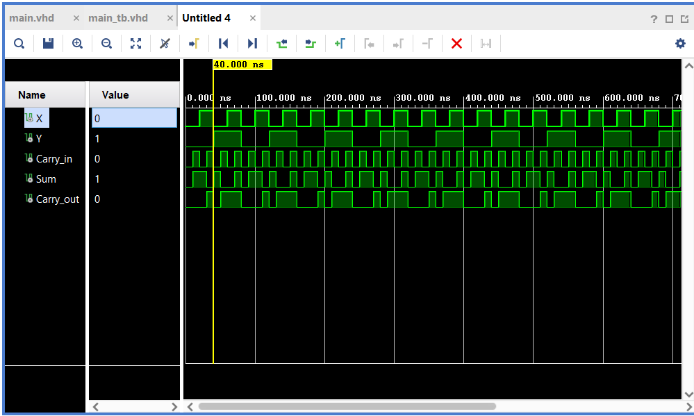
Now we are finished with our code! Let's take a look at the simulation.

Since there are so many test cases, there is a much more nuanced waveform. When we step through these waveforms, we see the result of our implementation is successful.